The OI!STER is an STM32L5 Target Board with a QFP48 clamshell socket aimed at debugging and glitching salvaged MCUs. The board can be powered via USB-C, a 2032 coin cell battery on the back of the board or an external power suppy. All pins are broken out in the 24-pin headers on either side at the top of the board. The OI!STER contains five debug headers, to support a wide range of debugging hardware such as a Hydrabus or a Black Magic Probe. It comes with six SMA connectors arranged in I/O pairs. One pair is dedicated to glitching the external LSE clock, another for glitching the external HSE clock and one pair for power analysis and fault injection with a Chipwhisperer. Each SMA connector can be bypassed by removing a small jumper. The OI!STER also has additional solder jumpers for the external clocks and each of the power traces to the MCU to allow for quick experimentation.
The Pinout diagrams below are directed at reverse engineering. The first diagram is targeted at debugging and reverse engineering an STM32L5 MCU itself. The second diagram is aimed at the communication between external peripherals and the MCU. Although some functionaly might overlap, we've found it practical to define these two pinout groups. Additional documentation is currently under development.
Debug Pinout Diagram
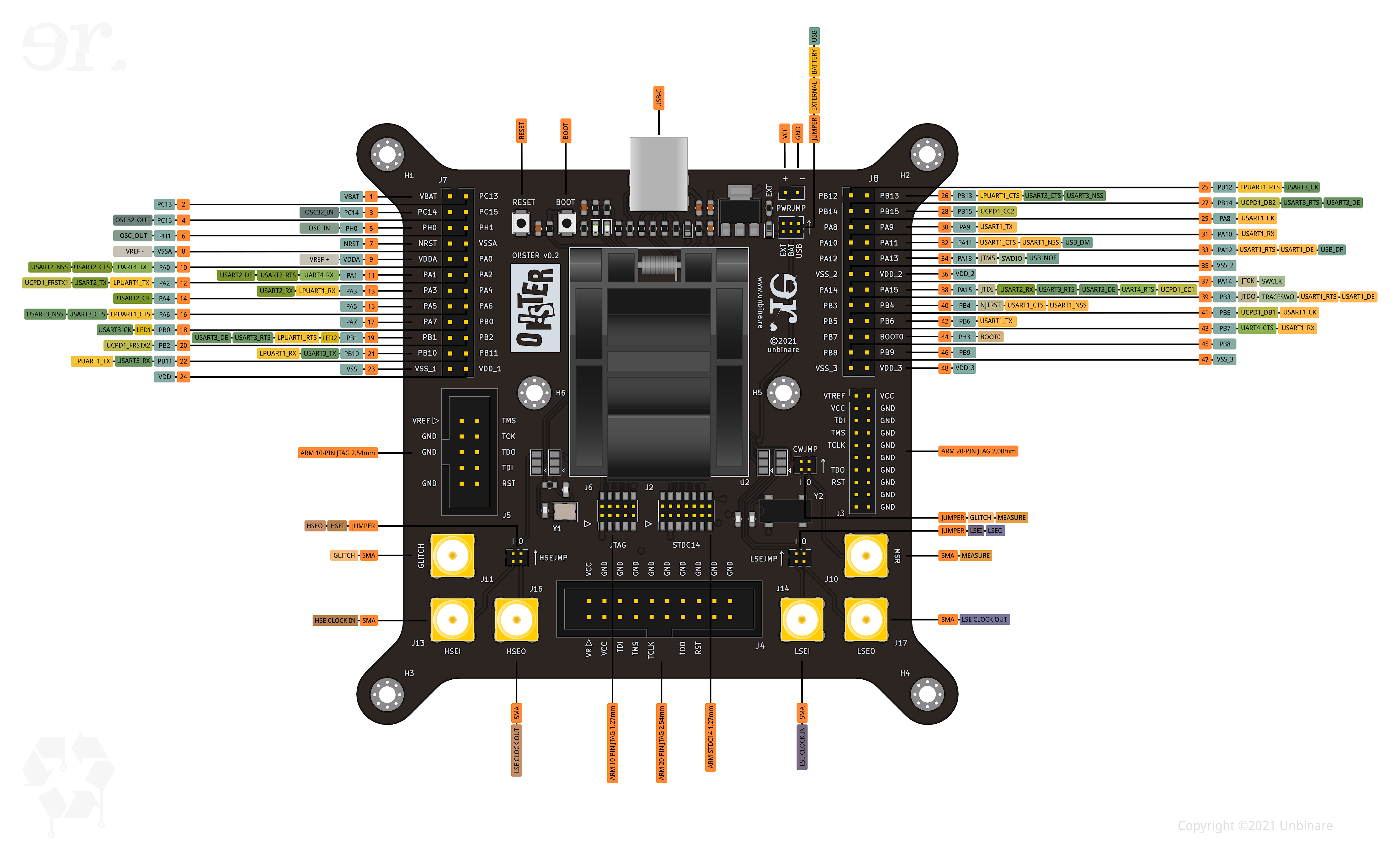
| Debug Pinout
|
| Pin
|
Function
|
Alternate Function
|
| 1
|
VBAT
|
| 2
|
PC13
|
| 3
|
PC14
|
OSC32_IN
|
| 4
|
PC15
|
OSC32_OUT
|
| 5
|
PH0
|
OSC_IN
|
| 6
|
PH1
|
OSC_OUT
|
| 7
|
NRST
|
| 8
|
VSSA
|
VREF-
|
| 9
|
VDDA
|
VREF+
|
| 10
|
PA0
|
UART4_TX
|
| 11
|
PA1
|
UART4_RX
|
| 12
|
PA2
|
LPUART1_TX
|
| 13
|
PA3
|
LPUART1_RX
|
| 14
|
PA4
|
USART2_CK
|
| 15
|
PA5
|
| 16
|
PA6
|
LPUART1_CTS
|
| 17
|
PA7
|
| 18
|
PB0
|
LED1
|
| 19
|
PB1
|
LED2
|
| 20
|
PB2
|
UCPD1_FRSTX2
|
| 21
|
PB10
|
USART3_TX
|
| 22
|
PB11
|
USART3_RX
|
| 23
|
VSS
|
| 24
|
VDD
|
| 25
|
PB12
|
LPUART1_RTS
|
| 26
|
PB13
|
LPUART1_CTS
|
| 27
|
PB14
|
UCPD1_DB2
|
| 28
|
PB15
|
UCPD1_CC2
|
| 29
|
PA8
|
USART1_CK
|
| 30
|
PA9
|
USART1_TX
|
| 31
|
PA10
|
USART1_RX
|
| 32
|
PA11
|
USART1_CTS
|
| 33
|
PA12
|
USART1_RTS
|
| 34
|
PA13
|
JTMS
|
| 35
|
VSS_2
|
| 36
|
VDD_2
|
| 37
|
PA14
|
JTCK
|
| 38
|
PA15
|
JTDI
|
| 39
|
PB3
|
JTDO
|
| 40
|
PB4
|
NJTRST
|
| 41
|
PB5
|
UCPD1_DB1
|
| 42
|
PB6
|
USART1_TX
|
| 43
|
PB7
|
UART4_CTS
|
| 44
|
PH3
|
BOOT0
|
| 45
|
PB8
|
| 46
|
PB9
|
| 47
|
VSS_3
|
| 48
|
VDD_3
|
Protocol Pinout Reference
| USB
|
| Pin
|
Function
|
Description
|
| 32
|
USB_DM
|
Data -
|
| 33
|
USB_DP
|
Data +
|
| 34
|
USB_NOE
|
Output Enable
|
| UCPD1
|
| Pin
|
Function
|
Description
|
| 12
|
UCPD1_FRSTX1
|
Fast Role Swap Signal
|
| 20
|
UCPD1_FRSTX2
|
Fast Role Swap Signal
|
| 27
|
UCPD1_DB2
|
Dead-Battery Signal
|
| 28
|
UCPD1_CC2
|
Configuration Control Line
|
| 38
|
UCPD1_CC1
|
Configuration Control Line
|
| 41
|
UCPD1_DB1
|
Dead-Battery Signal
|
| UART4
|
| Pin
|
Function
|
Description
|
| 10
|
UART4_TX
|
Transmit Data
|
| 11
|
UART4_RX
|
Receive Data
|
| 38
|
UART4_RTS
|
Request To Send
|
| 43
|
UART4_CTS
|
Clear To Send
|
| LPUART1
|
| Pin
|
Function
|
Description
|
| 12
|
22
|
LPUART1_TX
|
Transmit Data
|
| 13
|
21
|
LPUART1_RX
|
Receive Data
|
| 16
|
26
|
LPUART1_CTS
|
Clear To Send
|
| 19
|
25
|
LPUART1_RTS
|
Request To Send
|
| USART1
|
| Pin
|
Function
|
Description
|
| 29
|
41
|
USART1_CK
|
Transmitter Clock
|
| 30
|
42
|
USART1_TX
|
Transmit Data
|
| 31
|
43
|
USART1_RX
|
Receive Data
|
| 32
|
40
|
USART1_CTS
|
Clear To Send
|
| 32
|
40
|
USART1_NSS
|
Slave Select
|
| 33
|
39
|
USART1_RTS
|
Request To Send
|
| 33
|
39
|
USART1_DE
|
Driver Enable
|
| USART2
|
| Pin
|
Function
|
Description
|
| 10
|
|
USART2_CTS
|
Clear To Send
|
| 10
|
|
USART2_NSS
|
Slave Select
|
| 11
|
|
USART2_RTS
|
Request To Send
|
| 11
|
|
USART2_DE
|
Driver Enable
|
| 12
|
|
USART2_TX
|
Transmit Data
|
| 13
|
38
|
USART2_RX
|
Receive Data
|
| 14
|
|
USART2_CK
|
Transmitter Clock
|
| USART3
|
| Pin
|
Function
|
Description
|
| 16
|
26
|
|
USART3_CTS
|
Clear To Send
|
| 16
|
26
|
|
USART3_NSS
|
Slave Select
|
| 18
|
25
|
|
USART3_CK
|
Transmitter Clock
|
| 19
|
27
|
38
|
USART3_RTS
|
Request To Send
|
| 21
|
27
|
38
|
USART3_DE
|
Driver Enable
|
| 21
|
|
|
USART3_TX
|
Transmit Data
|
| 22
|
|
|
USART3_RX
|
Request Data
|
| JTAG
|
| Pin
|
Function
|
Description
|
| 34
|
JTMS
|
Test Mode State
|
| 37
|
JTCK
|
Test Clock
|
| 38
|
JTDI
|
Test Data In
|
| 39
|
JTDO
|
Test Data Out
|
| 40
|
NJTRST
|
Reset
|
| SWD
|
| Pin
|
Function
|
Description
|
| 7
|
NRST
|
Reset
|
| 34
|
SWDIO
|
Data I/O
|
| 37
|
SWCLK
|
Clock
|
| 39
|
TRACESWO
|
Trace Output
|
| OSC
|
| Pin
|
Function
|
Description
|
| 5
|
OSC_IN
|
High Speed External Clock In (HSEI)
|
| 6
|
OSC_OUT
|
High Speed External Clock Out (HSEO)
|
| OSC32
|
| Pin
|
Function
|
Description
|
| 3
|
OSC32_IN
|
Low Speed External Clock In (LSEI)
|
| 4
|
OSC32_OUT
|
Low Speed External Clock Out (LSEO)
|
Peripheral Pinout Diagram
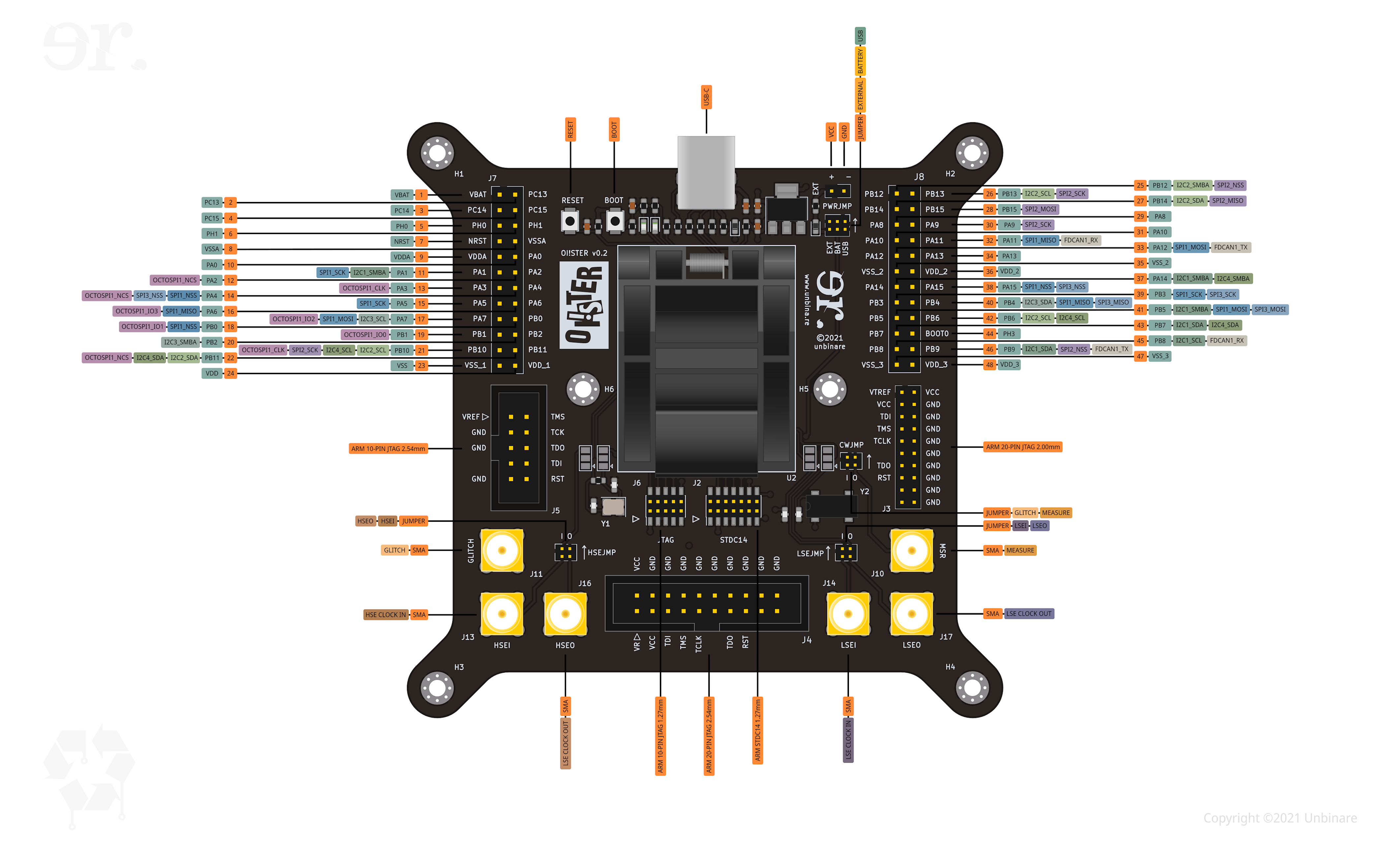
| Peripheral Pinout
|
| Pin
|
Function
|
Alternate
|
|
|
|
| 1
|
VBAT
|
| 2
|
PC13
|
| 3
|
PC14
|
| 4
|
PC15
|
| 5
|
PH0
|
| 6
|
PH1
|
| 7
|
NRST
|
| 8
|
VSSA
|
| 9
|
VDDA
|
| 10
|
PA0
|
| 11
|
PA1
|
I2C1_SMBA
|
SPI1_SCK
|
| 12
|
PA2
|
OCTOSPI1_NCS
|
| 13
|
PA3
|
OCTOSPI1_CLK
|
| 14
|
PA4
|
SPI1_NSS
|
SPI3_NSS
|
OCTOSPI1_NCS
|
| 15
|
PA5
|
SPI1_SCK
|
| 16
|
PA6
|
SPI1_MISO
|
OCTOSPI1_IO3
|
| 17
|
PA7
|
I2C3_SCL
|
SPI1_MOSI
|
OCTOSPI1_IO2
|
| 18
|
PB0
|
SPI1_NSS
|
OCTOSPI1_IO1
|
| 19
|
PB1
|
OCTOSPI1_IO0
|
| 20
|
PB2
|
I2C3_SMBA
|
| 21
|
PB10
|
I2C2_SCL
|
I2C4_SCL
|
SPI2_SCK
|
OCTOSPI1_CLK
|
| 22
|
PB11
|
I2C2_SDA
|
I2C4_SDA
|
OCTOSPI1_NCS
|
| 23
|
VSS
|
| 24
|
VDD
|
| 25
|
PB12
|
I2C2_SMBA
|
SPI2_NSS
|
OCTOSPI_NCLK
|
| 26
|
PB13
|
I2C2_SCL
|
SPI2_SCK
|
| 27
|
PB14
|
I2C2_SDA
|
SPI2_MISO
|
| 28
|
PB15
|
SPI2_MOSI
|
| 29
|
PA8
|
| 30
|
PA9
|
SPI2_SCK
|
| 31
|
PA10
|
| 32
|
PA11
|
SPI1_MISO
|
FDCAN1_RX
|
| 33
|
PA12
|
SPI1_MOSI
|
FDCAN1_TX
|
| 34
|
PA13
|
| 35
|
VSS_2
|
| 36
|
VDD_2
|
| 37
|
PA14
|
I2C1_SMBA
|
I2C4_SMBA
|
| 38
|
PA15
|
SPI1_NSS
|
SPI3_NSS
|
| 39
|
PB3
|
SPI1_SCK
|
SPI3_SCK
|
| 40
|
PB4
|
I2C3_SDA
|
SPI1_MISO
|
SPI3_MISO
|
| 41
|
PB5
|
I2C1_SMBA
|
SPI1_MOSI
|
SPI3_MOSI
|
| 42
|
PB6
|
I2C2_SCL
|
I2C4_SCL
|
| 43
|
PB7
|
I2C1_SDA
|
I2C4_SDA
|
| 44
|
PH3
|
| 45
|
PB8
|
I2C1_SCL
|
FDCAN1_RX
|
| 46
|
PB9
|
I2C1_SDA
|
SPI2_NSS
|
FDCAN1_TX
|
| 47
|
VSS_3
|
| 48
|
VDD_3
|
Protocol Pinout Reference
| I2C1
|
| Pin
|
Function
|
Description
|
| 11
|
41
|
I2C1_SMBA
|
System Management Bus Alert (SMBus mode)
|
| 43
|
46
|
I2C1_SDA
|
Serial Data Line
|
| 42
|
45
|
I2C1_SCL
|
Serial Clock Line
|
| I2C2
|
| Pin
|
Function
|
Description
|
| 21
|
26
|
I2C2_SCL
|
Serial Clock Line
|
| 22
|
27
|
I2C2_SDA
|
Serial Data Line
|
| 25
|
|
I2C2_SMBA
|
System Management Bus Alert (SMBus mode)
|
| I2C3
|
| Pin
|
Function
|
Description
|
| 17
|
I2C3_SCL
|
Serial Clock Line
|
| 25
|
I2C3_SMBA
|
System Management Bus Alert (SMBus mode)
|
| 40
|
I2C3_SDA
|
Serial Data Line
|
| I2C4
|
| Pin
|
Function
|
Description
|
| 21
|
42
|
I2C4_SCL
|
Serial Clock Line
|
| 22
|
43
|
I2C4_SDA
|
Serial Data Line
|
| 37
|
|
I2C4_SMBA
|
System Management Bus Alert (SMBus mode)
|
| SPI1
|
| Pin
|
Function
|
Description
|
| 11
|
15
|
39
|
SPI1_SCK
|
Serial Clock
|
| 14
|
18
|
38
|
SPI1_NSS
|
Slave Select
|
| 16
|
32
|
40
|
SPI1_MISO
|
Master-in, Slave-out
|
| 17
|
33
|
41
|
SPI1_MOSI
|
Master-out, Slave-in
|
| SPI2
|
| Pin
|
Function
|
Description
|
| 21
|
26
|
SPI2_SCK
|
Serial Clock
|
| 25
|
|
SPI2_NSS
|
Slave Select
|
| 27
|
|
SPI2_MISO
|
Master-in, Slave-out
|
| 28
|
|
SPI2_MOSI
|
Master-out, Slave-in
|
| SPI3
|
| Pin
|
Function
|
Description
|
| 14
|
38
|
SPI3_NSS
|
Slave Select
|
| 39
|
|
SPI3_SCK
|
Serial Clock
|
| 40
|
|
SPI3_MISO
|
Master-in, Slave-out
|
| 41
|
|
SPI3_MOSI
|
Master-out, Slave-in
|
| OCTOSPI1
|
| Pin
|
Function
|
Description
|
| 12
|
14
|
OCTOSPI1_NCS
|
Chip Select
|
| 13
|
21
|
OCTOSPI1_CLK
|
Clock
|
| 16
|
|
OCTOSPI1_IO3
|
I/O Data Line
|
| 17
|
|
OCTOSPI1_IO2
|
I/O Data Line
|
| 18
|
|
OCTOSPI1_IO1
|
I/O Data Line
|
| FDCAN
|
| Pin
|
Function
|
Description
|
| 32
|
45
|
FDCAN_RX
|
Receive Data
|
| 33
|
46
|
FDCAN_TX
|
Transmit Data
|


