UNBRK: Difference between revisions
Unbinawiki (talk | contribs) No edit summary Tags: mobile web edit mobile edit |
Unbinawiki (talk | contribs) mNo edit summary |
||
| Line 8: | Line 8: | ||
== '''Pinout:''' == | == '''Pinout:''' == | ||
{| class="wikitable | {| class="wikitable" | ||
|- | |- | ||
! Pinout | ! Pinout | ||
Revision as of 14:24, 22 July 2021
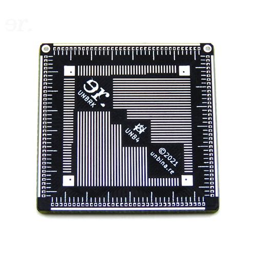
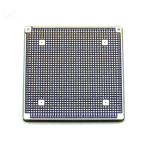
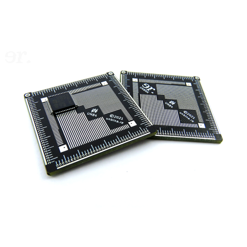
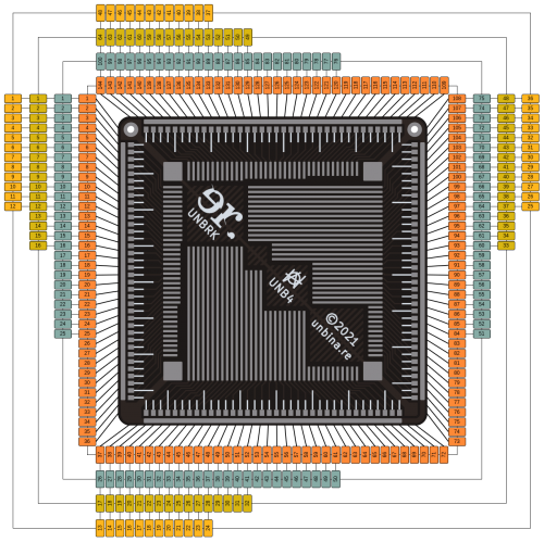
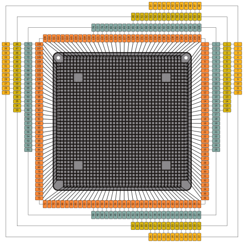
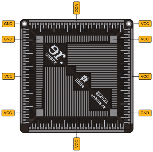
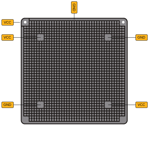
UNBRK is a 3.2x3.2cm QFP48/64/100/144 breakout board with a VCC bus on all four edges of the topside of the board and a GND bus on all four edges on the bottom of the board. The buses have been placed adjacent to the breakout pads to simplify the process of powering the MCU and the placement of decoupling capacitors where this might be necessary. Due to the board being as small as it is, we've added ruler lines to the breakout pads on the top of the board to ease finding the correct pin numbers when using the pinout diagrams on this page. The remaining area on the bottom of the UNBRK functions as a prototyping area for 0201-sized surface-mount components. The aim of the project is to allow rapid prototyping with MCUs by using components salvaged from discarded mobile phones. Full documentation is currently under development.
Pinout:
| Pinout |
|---|
|
|
|
|
