DEDBUG Protoboard: Difference between revisions
Unbinawiki (talk | contribs) |
Unbinawiki (talk | contribs) |
||
| Line 44: | Line 44: | ||
=='''DEDBUG Protoboard Diagram [Back]'''== | =='''DEDBUG Protoboard Diagram [Back]'''== | ||
<br><br> | <br><br> | ||
<gallery widths="750px" heights="750px" mode=" | <gallery widths="750px" heights="750px" mode="nolines"> | ||
Image:DEDBUG plot back description 50.png | Image:DEDBUG plot back description 50.png | ||
</gallery> | </gallery> | ||
Revision as of 17:02, 28 June 2023
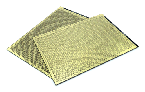
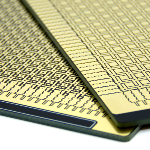
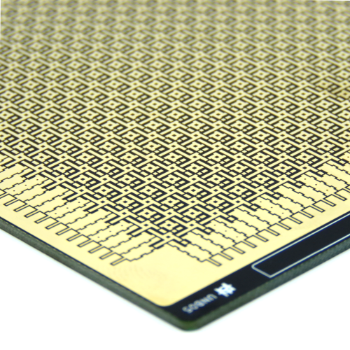
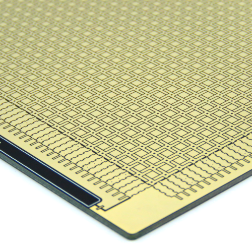
DEDBUG is a protoboard aimed at deadbug prototyping and free-form circuit construction with components salvaged from electronic waste. Unlike traditional perfboards and stripboards, the main objective of this protoboard is to provide a means to work with SMD components. Since founding the lab in 2020, due to the influence of the manufacturing industry on the hardware hacking community we have observed a gradual decline in manual experimentation and prototyping with SMD components in favour of establishing small-scale production pipelines with desktop CNC routers, pick-and-place machines and reflow ovens and other costly production-oriented equipment. We find that this trend loosely mirrors production processes in larger production pipelines, aimed at commercially producing and selling devices. At Unbinare, we would like to preserve the unpremeditated, spur-of-the-moment nature of hardware hacking and openly share the skills required to manually hack free-form circuits with SMD components. The DEDBUG protoboard is designed to allow anyone to experiment and build free-form circuits with relative ease and demonstrates that with few resources one is able to modify and repurpose discarded electronic devices instead of creating new products. The project has been supported by Constant VZW as part of their TechnoDisobedience Project. They generously provided the resources for the design, production and the organization of the first DEDBUG workshop. Further development of the project is supported by NLnet and the NGI Zero Fund as part of the Reverse Engineering Toolkit project. Additional documentation is currently under development.
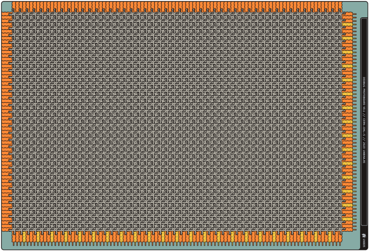
DEDBUG Protoboard Diagram [Front]
| Color | Function | Description |
|---|---|---|
| Bus | A bus on the right and bottom edge of the Protoboard. On the top right edge of the Protoboard it is possible to solder a wire or attach a crocodile clip to create either a VCC or GND Bus. | |
| Edge Pads | The edge pads can be bridged with the Bus, bridged to adjacent edge pads and bridged with the prototyping area. It is possible to bridge with just solder, or an 0402-sized zero-ohm resistor. | |
| Edge Pads [Vias] | These edge pads connect to their corresponding pads on the other side using vias. If one side has a VCC Bus and the other the GND bus, it is possible to complete a circuit by bridging an edge pad with vias on the relevant side so both buses are available to the prototyping area. | |
| Prototyping Area | This prototyping area has been designed to both accommodate building circuits with magnet wire or without any wire at all by bridging the cross-shaped pads. Since two-terminal SMD components can be difficult to solder using freeform prototyping techniques,
the prototyping grid allows for the most common (0201/0402/0603/0805/1206/1210) two-terminal SMD components. A guide will be created in a future iteration of this wiki page. |
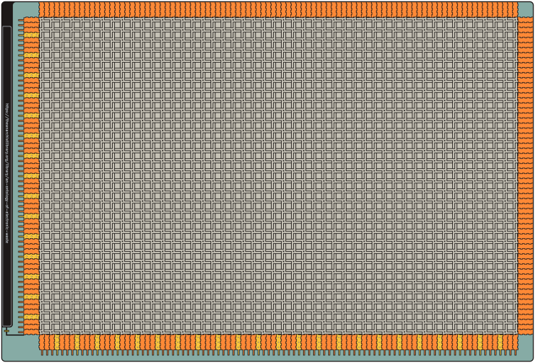
DEDBUG Protoboard Diagram [Back]
| Color | Function | Description |
|---|---|---|
| Bus | A bus on the right and bottom edge of the Protoboard. On the top right edge of the Protoboard it is possible to solder a wire or attach a crocodile clip to create either a VCC or GND Bus. | |
| Edge Pads | The edge pads can be bridged with the Bus, bridged to adjacent edge pads and bridged with the prototyping area. It is possible to bridge with just solder, or an 0402-sized zero-ohm resistor. | |
| Edge Pads [Vias] | These edge pads connect to the edge pads on the other side using vias. If one side has a VCC Bus and the other the GND bus, it is possible to complete a circuit by bridging an edge pad with vias on the relevant side so both buses are available to the prototyping area. | |
| Prototyping Area | This prototyping area has been designed to both accommodate building circuits with magnet wire or without any wire at all by bridging the cross-shaped pads. Slightly different from the prototyping area found on the front of the Protoboard,
This side accommodates building zones and makes it easier to attach DEDBUG ProtoFlex PCBs. | |
| Bridge Guard | The function of this small pad is to prevent accidental shorting the buses on opposite sides of the board when using crocodile clips. It is not possible to use solder to bridge, as the surface tension of the solder and the shape of the area prevents it.
The best way to bridge the two buses on the left and bottom sides of the board is to cut off a 2x2mm piece of solder wick and solder it on top of the bridge guard. |
