OI!STER: Difference between revisions
Unbinawiki (talk | contribs) No edit summary |
Unbinawiki (talk | contribs) No edit summary |
||
| Line 6: | Line 6: | ||
[[File:OISTER-30.png|center|750px]] | [[File:OISTER-30.png|center|750px]] | ||
[[File:OISTER-PCB-30.png|center|750px]] | [[File:OISTER-PCB-30.png|center|750px]] | ||
<br><br> | |||
== '''Pinout''' == | |||
{| class="wikitable" | |||
|+ | |||
! Pinout | |||
|- | |||
| [[File:OISTER Pinout-50.png|500px]] | |||
|} | |||
Revision as of 22:31, 22 July 2021
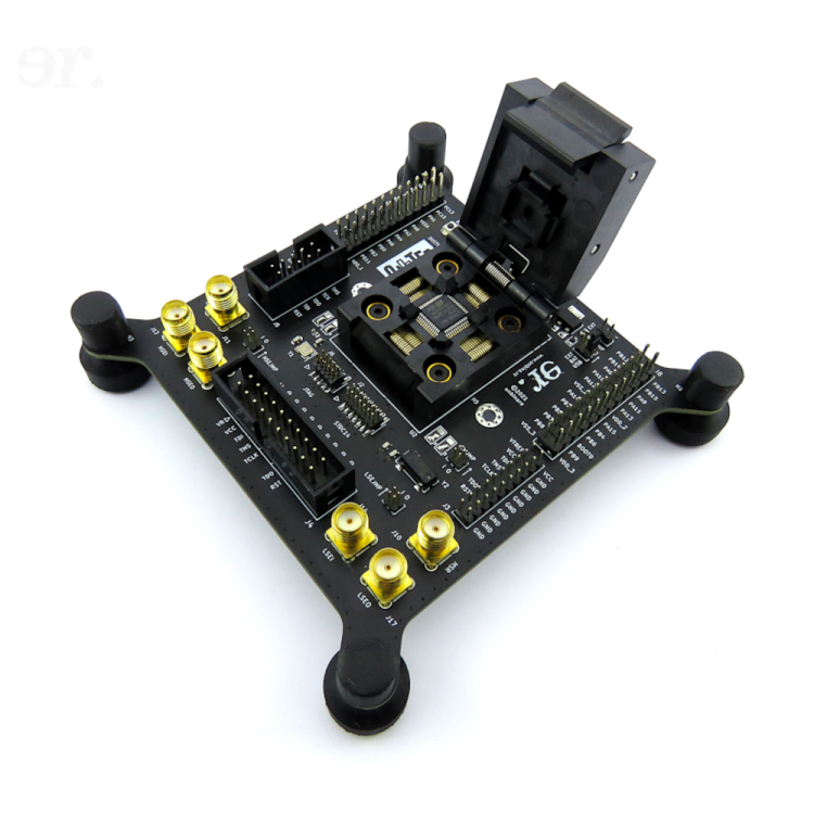
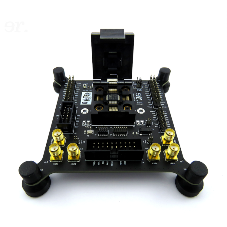
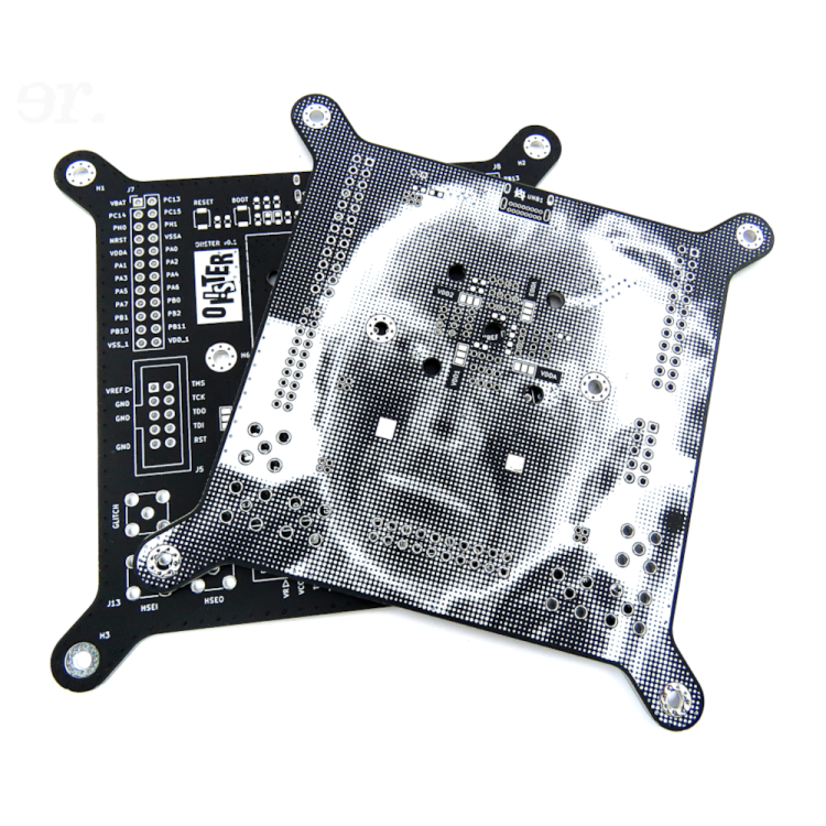
The OI!STER is an STM32L5 Target Board with a QFP48 clamshell socket aimed at debugging and glitching salvaged MCUs. The board can be powered via USB-C, a 2032 coin cell battery on the back of the board or an external power suppy. All pins are broken out in the 24-pin headers on either side at the top of the board. The OI!STER contains five debug headers, to support a wide range of debugging hardware such as a Hydrabus or a Black Magic Probe. It comes with six SMA connectors arranged in I/O pairs. One pair is dedicated to glitching the external LSE clock, another for glitching the external HSE clock and one pair for power analysis and fault injection with a Chipwhisperer. Each SMA connector can be bypassed by removing a small jumper. The OI!STER also has additional solder jumpers for the external clocks and each of the power traces to the MCU to allow for quick experimentation.
A full pinout and additional documentation is currently under development.
Pinout
| Pinout |
|---|
| File:OISTER Pinout-50.png |


